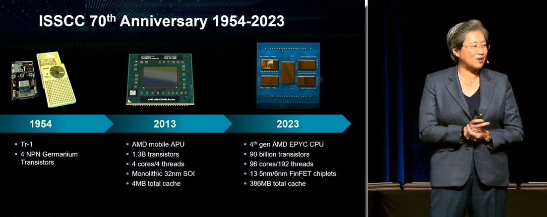
As a prelude to the ISSCC conference in San Francisco at the end of February, AMD CEO Lisa Su had the honour of opening the proceedings. She did so in the form of a warning : our growing dependence on high-performance computing will not be sustainable from an energy point of view without enormous progress in the consumption of the chips involved. “Even if Moore’s Law has slowed down, supercomputer performance tends to double every 1.2 years, which is at least twice as fast as the progress made in energy efficiency. At this rate, we could be looking at zettascale supercomputers in less than ten years, but each one would require 500 MW to power it, the equivalent of half a nuclear power station“, explains Lisa Su. This is obviously neither sustainable nor desirable. Fortunately, there are ways of keeping chip consumption within more reasonable limits.
According to AMD’s CEO, the first task lies in the assembly and encapsulation of integrated circuits. It is no longer possible to rely solely on the reduction of lithography geometries to improve the chips efficiency : “progress slowed down from 7 nm in terms of density, and stopped from 5 nm onwards in terms of thermal efficiency“. In addition, production costs are soaring for large chips produced in advanced technologies. Finally, despite their progress, memory and I/O performance are struggling to keep pace with miniaturisation. Hence the advent of modular architectures combining multiple chiplets in a single package. Not only does this layout optimise the process for each function (memory, digital processing, I/O, etc.), but it also brings the different elements physically closer together, making interconnections much more frugal. Yet modern components often spend as much energy carrying data as processing it. “Fetching a bit from memory consumes about as much energy as performing a 64-bit floating point operation“, notes Lisa Su. The advent of 2.5D encapsulation technologies, often involving an interposer layer, is of great service here. Stacking chips in three-dimensional packages offers further gains, as demonstrated by HBM memories that combine higher bandwidth than DDR5 Dram with three to four times lower power consumption per bit. “But true 3D assembly methods for heterogeneous chips are still in their infancy and need to mature“, adds Lisa Su. Stacking chips poses challenges in terms of heat dissipation, and the interfaces of the different elements need industry-wide standards (such as those promoted by the UCLe initiative) to facilitate their dialogue. “In a way, the package has become the new motherboard ; thanks to widely accepted interconnection standards, each manufacturer will be able to optimise its part of the system“, prophesies Lisa Su.
Another method of making better use of memory and limiting data round trips is processing in memory (PIM), a technique that is “a bit counter-intuitive for us processor manufacturers“, says the AMD CEO with a smile, but which is the subject of a great deal of research and which was also the subject of a separate presentations category at ISSCC 2023. Another priority for the future : processors and complex circuits will have to be equipped with integrated optical interfaces so that the energy efficiency efforts undertaken inside the package are not wasted by the increased consumption linked to the transport of this data. Lisa Su is also betting on the advent of standardised interfaces in this area, for example around the CXL protocol, and cites the presentation by an AMD team of an optical WDM link consuming a total of 2.5 pJ/bit and made by stacking 7 nm Cmos and 45 nm optical chips.
Finally, Lisa Su praised in San Francisco the use of dedicated accelerators within the circuits. It is no longer a question of processing all the algorithms at the level of rarely optimised software code, relying on super-powerful processors: energy constraints impose more than ever a sort of return to hardware processing, which has already considerably increased the functionality of our smartphones, for example. “This is especially true in artificial intelligence processing, where new data formats with reduced precision need to be natively supported by processors to improve their efficiency“, explains Lisa Su. To bring things full circle, this AI, which is advancing much faster than conventional digital processing, is also beginning to significantly improve the design of the chips themselves. “In a study using Synopsys’ DSO.ai technology, we found that AI-backed CAD tools outperformed the best engineering teams for some tasks, and this will intensify as AI becomes involved in all stages of circuit design“, says Su. Will all this be enough to achieve zettascale performance in a 100 MW thermal envelope? At least that’s the AMD executive’s goal.


